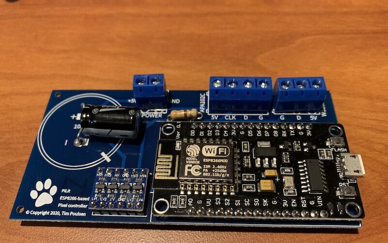
PCB design is complicated and necessitates careful preparation, regardless of whether you use a PCB computer-aided design or assemble one by hand. In order for a PCB to work properly, it must take into account a wide range of variables. These six steps are a great way to deal with all of these issues at once.
- Draw Or Generate A Circuit Schematic
The first step is to begin designing your PCB, either by hand or with the aid of a computer. First, figure out the circuit you would like to design before you start wiring things up. As a result, a schematic is required, whether from scratch or from someone else’s design. Note that spacing matters. Optimal spacing increases efficiency while reducing signal resistance and overheating.
- Customize the Board Layout
It’s time to put pencil to paper. Using your schematic diagram, you’ll need to create a drawing of your PCB. This isn’t as difficult as it may appear at first glance. The software compares your design to a schematic file, enabling you, as a result, to make similar connections. The component’s footprint is an essential consideration in this decision. Surface mount or through-hole?
Soldering through-hole components is the simplest. Starting out, go for a through-hole. Due to their tiny size, surface-mount components save a significant amount of space. Smaller, though, can make soldering more difficult. Surface-mounted components, on the other hand, can be mastered with a little practice. It’s up to you if you’re up for it.
To get the best results, spend some time on it. Draw circuit boards in accordance with the design criteria.
- Begin With the Components
The quality of your PCB’s construction and design can be substantially enhanced by starting with the placement of your components. By starting with the components, you’re ensuring that your PCB is capable of doing the tasks you’ve set out for it. Keep in mind the emphasis on spacing.
- Pay Attention to the Traces
Each component of a PCB is linked together by traces. Without them, the board’s signals won’t be able to go through it. You should try to make all of your traces short and direct, minimizing signal travel time and space. When you’re spacing your traces, keep in mind radio frequency interference as well as resistance.
- Watch Out for Overheating
This is the final important phase in the design of a PBC. Materials and part spacing have a significant role in this. Overheating can be reduced by drilling holes and vias in your board.
- Prototyping and Manufacturing of PCBs
It’s time to start making your PCB after your design layout is perfect. A full line of PCBs can benefit greatly from PCB fabrication services, but prototype PCBs can be made to test your design first. Working with an experienced service provider for PCB manufacturing means that any problems that may arise can be dealt with quickly and effectively.
Making a custom PCB in this manner can assist in streamlining your design process. If you follow this advice, your initiatives should go off without a hitch. PCB prototyping is a great way to test your design before you commit to a full production run.
ChinaPCBOne Technology LTD. is the author of this article on PCB fabrication. Find more information, about PCB manufacturing.


